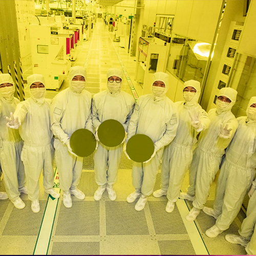
Samsung to start producing 3nm chips for servers

According to sources, Samsung Foundry will begin producing HBM (High Bandwidth Memory) server-grade SiPs (System-in-Packages) for an unidentified US client. The South Korean company, AD Technology designed the chip. It uses 2.5D packaging technology and HBM memory. Furthermore, it is unknown if Samsung Foundry is fabricating the chip using the SF3E (first-generation 3nm fabrication method) or the SF3 (second-generation 3nm process).
Jeong Ki-bong, Vice President of the Business Development Team at Samsung Electronics Foundry Division, said, “We are pleased to be able to announce this 3-nano design collaboration with AD Technology. This project will set a good precedent in the cooperation program between Samsung Electronics Foundry Division and ecosystem partners. “Samsung Electronics Foundry Division will strengthen cooperation with partners to provide the best quality to customers.”
Samsung Foundry started making 3nm chips a few months before TSMC, but it could not get the big-name clients like AMD, Apple, MediaTek, Nvidia, and Qualcomm. Recently, Apple has announced the A17 Pro chip which is made using TSMC's 3nm process. It is expected that Samsung’s second-generation 3nm process (SF3) will be available early next year and it allows varying nanosheet channel widths within the same cell type, offering improved power, performance, and area compared to SF3.
In 2025, Samsung Foundry is expected to ready SF3P, its third-generation 3nm chip fabrication process with performance enhancements. This process can be used to make server and smartphone chips.
See What’s Next in Tech With the Fast Forward Newsletter
Tweets From @varindiamag
Nothing to see here - yet
When they Tweet, their Tweets will show up here.


