Hero Electronix's Tessolve inaugurates Chip Design Center of Excellence

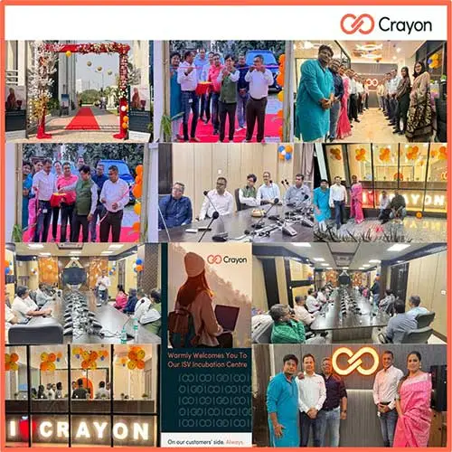
Hero Electronix has announced the opening of its dedicated Semiconductor Chip Design Center in Bengaluru. The center has been set up by Tessolve, a Hero Electronix venture and a leading engineering solutions company. The center will focus on the needs of Tessolve’s clients, which include major global semiconductor companies. The company recently inaugurated another center in Visakhapatnam, which primarily focuses on software and test program development. The goal is to scale the design team by 100% over the next two years to support the growing demand for chip design projects from Tessolve’s customers.
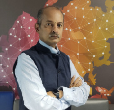
P. Raja Manickam, Founder & CEO, Tessolve, says, “Our vision is to be the leader in semiconductor and systems engineering from concept to delivering chips and systems. We believe in being a technology services company where we help our customers with in-depth expertise, enable time-to-market advantage and economic benefits. It is an important milestone for the Tessolve team in our journey to become a chip design leader and is followed by the acquisition of Analog Semiconductors a year back to strengthen our analog design capabilities. It will further help in strengthening our capabilities as an end-to-end solutions partner and semiconductor engineering services leader.”
The new design center will provide strong impetus to Tessolve’s chip design offering. As more and more clients seek capability and depth in a critical area like chip design, a new facility has been set up as the center of excellence for all chip design projects. It will work in close association with Tessolve’s other design centers to develop innovative chip solutions across verticals – automotive, server, graphics and mobile platforms, to name a few. Training will be a key focus area. Tessolve already runs training programs for engineering talent aimed at long-term growth and development of the workforce.
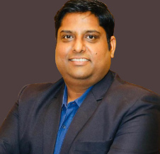
Nikhil Rajpal, CEO, Hero Electronix, says, “We are proud of Tessolve’s growth and achievement since our partnership as today it is amongst the leaders in the semiconductor engineering space. We have not been shy of making investments in assets and infrastructure to add strategic capabilities as Tessolve made acquisitions in the key areas – embedded systems, analog design, PCB fabrication and test lab. The new design centre will help accelerate Tessolve’s growth and replicate its test engineering leadership in chip design.”
The new center is located at Global Technology Park, Block C, Bellandur, Outer Ring Road. The new office will be catering to chip design projects across all domains – Design Verification, Design for Test and Debug, Physical Design, FPGA Emulation, Post SI Validation, Analog & Mixed Signal (AMS) Design.
See What’s Next in Tech With the Fast Forward Newsletter
Tweets From @varindiamag
Nothing to see here - yet
When they Tweet, their Tweets will show up here.


